Micro- and nanofabrication
Surface nanostructuring
Several laser-based techniques enable precise micro- and nanostructuring of metal, semiconductor, glass, and other material surfaces.
Introduction
What surface nanostructuring covers
Nanotechnology and lasers are among the most successful and active fields of research and technology in the past decades and provide great potential when merged together. Several laser-based techniques enable surface nanostructuring of metal, semiconductor, or even glass, which are then employed in sensing, imaging, solar energy, and biomedicine. Such laser-based techniques include but are not limited to the formation of laser-induced periodic surface structures (LIPSS), laser interference lithography (LIL), and direct laser interference patterning (DLIP).
LIPSS
Formation of LIPSS, also known as ripples or nanoripples, is a direct laser writing technique for manufacturing grating-like nanostructures. LIPSS originate from the interference of the incident/refracted laser light with the scattered or diffracted light near the surface. The technique has gained a lot of interest due to its simplicity and robustness as its manufacturing can be performed in ambient air and is fully compatible with industrial demands on costs, reliability, and productivity. Depending on the selected materials and irradiation conditions, the processing of LIPSS enables various types of surface functionalization through different periods, ranging from a few tens of nanometers to several micrometers.
LIL and DLIP
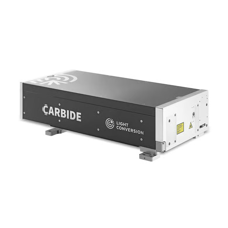
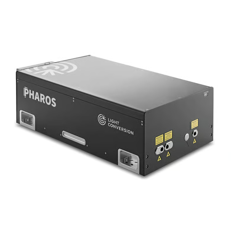
LIL and DLIP rely on the laser interference of incident laser light. Two or more laser beams are superimposed in the spatial and temporal domain, creating an interference pattern with its period down to a subwavelength scale. In LIL, the pattern is first recorded in a light-sensitive medium and then transferred into the material of interest. On the contrary, DLIP enables a direct structuring of material. At the right irradiation conditions, the surface gets melted or even ablated at the peaks of intensity. Given the inherently large spectral bandwidth of ultrashort laser pulses and its impact on the resulting interference patterns, the LIL and DLIP techniques are often limited to pulse durations in the ps-range or longer. However, this is not an issue with the tunability of pulse duration up to 20 ps – a feature of CARBIDE and PHAROS femtosecond lasers.
Choosing a technique
When choosing the technique, several aspects have to be considered. In LIL and DLIP, the period of the interference pattern is controlled by the wavelength of laser irradiation and the angle of incidence between the interfering beams. However, the minimum period is limited by the optical diffraction limit. Thus, if a sub-100 nm feature size is desired, one should go with LIPSS. Another aspect is the modulation depth of the nanostructured pattern. The depth of the DLIP pattern can be independently controlled by the laser pulse energy and the number of pulses applied. Even though a similar relation is expected for LIPSS, it is typically more difficult to control. DLIP structures can have significantly larger modulation depths and regularity over a large area.
SERS sensor fabrication
SERS sensor fabrication. SEM image of the Ti-6Al-4V (TC4) surface after irradiation with a progressive laser scan.
Where nanostructured surfaces are used
The nanostructured surfaces are widely used in sensing, e.g., surface-enhanced Raman spectroscopy (SERS), where a roughened metallic surface enhances the Raman scattering of the adsorbed analyte molecules by several orders of magnitude. Also, nanostructured materials, such as black silicon, have found interest in photodetectors and solar cells. The micrometric silicon spikes trap the incident light, subsequently providing high absorptance in the visible and infrared spectral ranges. Furthermore, LIPSS and other nanostructuring techniques enable hydrophobic and hydrophilic surfaces for automotive and aerospace engineering, antibacterial and cell-repellent or cell-stimulating surfaces for medical applications, and many other applications. CARBIDE and PHAROS femtosecond lasers are widely used for these surface nanostructuring techniques.