Micro- and nanofabrication
Color center formation
Femtosecond laser writing enables the writing of vacancy-related color centers in silicon carbide and gallium nitride, which are relevant for applications in quantum technologies.
Introduction
Laser-written color centers
Illustration of the laser writing of color centers (left), silicon carbide containing arrays of laser-written color centers (right). Courtesy of RMIT University, Melbourne.
Why color centers matter
Color centers in wide bandgap semiconductors are relevant for quantum technologies as they can produce single-photon sources or be used as spin qubits and in quantum sensing applications. Femtosecond laser writing enables vacancy-related color center formation in silicon carbide (SiC) and gallium nitride (GaN), giving rise to photoluminescence from the visible to the infrared range.
How the color is formed
The process of color center formation involves point defects or point defect clusters associated with trapped electrons or holes in ordinarily transparent materials. When the electron ground state of the defect is excited to higher energy states by the absorption of laser light, these centers cause the solid to become colored.
SiC arrays written with PHAROS
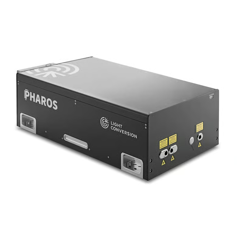
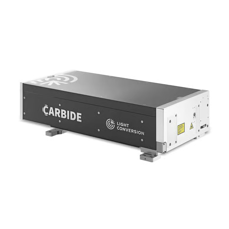
Using a PHAROS laser with a 515 nm wavelength and 230 fs pulse duration, RMIT University scientists produced large arrays of silicon-vacancy defects in SiC with high localization within the confocal diffraction limit of 500 nm and minimal material damage. The number of color centers formed exhibited power-law scaling with the laser fabrication energy, indicating that photoinduced ionization creates the color centers. Color center arrays play a crucial role in quantum applications. Both CARBIDE and PHAROS femtosecond lasers can be applied to generate color centers in wide bandgap semiconductors.